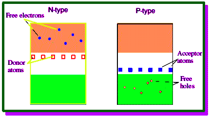
To understand PN junction diode , consider two separate pieces of semi conductors (p-type and n-type ) as shown in below figure
There are two operating regions and three possible “biasing” conditions for the standard Junction Diode and these are:
- 1. Zero Bias(UNBIASED) – No external voltage potential is applied to the PN junction diode.
- 2. Forward Bias – The voltage potential is connected positive to the P-type material and negative to the N-type material across the diode.
- 3. Reverse Bias – The voltage potential is connected negative to the P-type material and positive to the N-type material across the diode.
- PN Junction Diode in Equilibrium with No Applied Voltage(UNBIASED)
1.A diode is made of semiconductor material (such as crystalline silicon) with impurities added in a process called doping. Different impurities are added to the anode and cathode sides to make the diode electrically asymmetric.
2.The semiconductor on the anode side is doped with atoms having 3 valence electrons each (such as indium, aluminum or gallium). Relative to pure silicon which has 4 valence electrons, it has a deficit of electrons and these missing electrons are called holes. A semiconductor doped in this way is called p-type, where the “p” stands for the positively-charged holes
3.The semiconductor on the cathode side is doped with atoms having 5 valence electrons each (such as phosphorus or arsenic) and, thus, has an excess of electrons relative to pure silicon. This kind of doped semiconductor is called n-type because the excess electrons are negatively charged.
5. If one half is doped by P-type impurity and the other half is doped by N-type impurity, a PN junction is formed.
6. The semicondctor dividing the two halves is called PN junction. The N-type material has high concentration of free electrons, while P-type material has high concentration of holes.
7. Therefore, at the junction there is a tendency for the free electrons to diffuse over to the P-side and holes to the N-side.This process is called diffusion.
8. As the free electrons move across the junction from N-type to P-type, the donor ions become positively charged. Hence a positive charge is built on the N-side of the junction. The free electrons that cross the junction uncover the negative acceptor ions by filling in the holes.
9. Therefore, a net negative charge is established on the P-side of the junction.
10. This net negative charge on the P-side prevents further diffusion of electrons into the P-side. Similarly, the net positive charge on the N-side repels the hole crossing from P-side to N-side.
11. Thus a barrier is set-up near the junction which prevents further movement of charge carriers. i.e. electrons and holes.
12. As a consequence of the induced electric field across the depletion layer, an electrostatic potential difference is established between P-and N-regions, which is called the potential barrier, junction barrier, diffusion potential, barrier potential,space charge region or contact potential.


