Saturday, November 15, 2014

PN JNCTION DIODE V-I CHARACTERISTICS

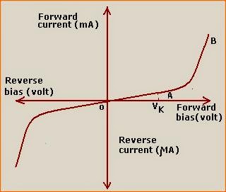
1.The response of PN junction diode can be easily indicted with the help of characteristics called V-I characteristics.

2.It is the graph drawn between applied voltage across the diode and the current flowing through the diode.

CHARACTERISTICS OF A DIODE:
     
         Under forward bias condition, the applied voltage is denoted by Vf  and forward current flowing is denoted by If  .The graph Vf  vs If is called forward characteristics of a pn junction diode.

        In forward bias condition as long as forward voltage is less than barrier potential ,there is no forward current.Once forward voltage greater than barrier potential , the forward current starts flowing,the current increases drastically.

        Under reverse bias condition, the applied voltage is denoted by Vr  and a small reverse satration current flowing is denoted by Io  .The graph Vr  vs Ir is called reverse characteristics of a pn junction diode.

pn diode characteristics


Monday, August 4, 2014

PN JNCTION DIODE UNDER REVERSE BIAS

pn junction under reverse bias


1.When the pn junction is reverse biased the negative teriminal attracts the holes in the p region, away from the junction.

2.The positive terminal attracts the free electrons in the n region away from the junction.

3.No charge carrier is able to cross the junction.As electrons and holes both move away from the junction, the depletion region widens.

4.As depletion region widens, barrier potential across the junction also increases.

5.The positive side drags the electrons from p region towards the positive of battery.Similarly negative side of barrier potential drags the holes from n region towards the negative of battery.

6.The electrons on p side and holes on n side are minority charge carriers,which constitute the current in reverse biased condition.Thus reverse conduction takes place

7.The reverse current flows due to minority charge carriers which are small in number.Hence reverse current is always very small.This reverse current is called reverse saturation current.

pn junction diode reverse bias

reverse biased pn junction diode


PN JNCTION DIODE UNDER FORWARD BIAS


BIASING: Applying external d.c voltage to any electronic device is called  biasing.

     If an external voltage is applied in such a way that the p type semiconductor is connected to the positive terminal  of the dc voltage and the n type semiconductor to the negative terminal of the dc voltage.

pn junction diode forward bias

diode forward biased
Add caption
OPERATION OF FORWARD BIASED DIODE:
pn junction diode forward bias
Add caption

forward biased pn junction

1.When the pn junction is forward biased as long as the applied voltage is less than the barrier potential ,there is no current flow(conduction).

2.When the applied voltage becomes more than the barrier potential,the negative terminal repels the free electrons against barrier potential from n to p region.

3.similarly positive terminal repels the free holes against barrier potential from p to n region and cross the junction.

4.Thus the applied voltage overcomes the barrier potential.This reduces the width of depletion region.

5.As forward voltage increased,at a particular value the depletion region becomes very much narrow  such that large number of majority carriers can cross the junction.

6.The large number of majority carriers constitute a current called forward current.

7.The overall forward current is due to the majority charge carriers.

8.These majority carriers can then travel around the closed circuit and a relatively large current flows.

9.The direction of flow of electrons is from negative to positive of the battery.

10.While the direction of the conventional current is from positive to negative of the battery.


Sunday, August 3, 2014

SYMBOL OF DIODE

DIODE SYMBOL
        The p region acts as anode while the n region acts as cathode.The 

arrow in the symbol indicates the direction of the conventional current.


Tuesday, July 29, 2014

PN JUNCTION DIODE(unbiased)


To understand PN junction diode , consider two separate pieces of semi conductors (p-type and n-type )  as shown in below figure

pn diode

Bring p-type and n-type semi conductors together and join them to make pn junction diode as shown in figure below.
pn junction diode
There are two operating regions and three possible “biasing” conditions for the standard Junction Diode and these are:

  • 1. Zero Bias(UNBIASED) – No external voltage potential is applied to the PN junction diode.
  • 2. Forward Bias – The voltage potential is connected positive to the P-type material and negative to the N-type material across the diode.

  • 3. Reverse Bias – The voltage potential is connected negative to the P-type material and positive to the N-type material across the diode.
  • PN Junction Diode in Equilibrium with No Applied Voltage(UNBIASED)
1.A diode is made of semiconductor material (such as crystalline silicon) with impurities added in a process called doping. Different impurities are added to the anode and cathode sides to make the diode electrically asymmetric.

2.The semiconductor on the anode side is doped with atoms having 3 valence electrons each (such as indium, aluminum or gallium). Relative to pure silicon which has 4 valence electrons, it has a deficit of electrons and these missing electrons are called holes. A semiconductor doped in this way is called p-type, where the “p” stands for the positively-charged holes
3.The semiconductor on the cathode side is doped with atoms having 5 valence electrons each (such as phosphorus or arsenic) and, thus, has an excess of electrons relative to pure silicon. This kind of doped semiconductor is called n-type because the excess electrons are negatively charged.

5. If one half is doped by P-type impurity and the other half is doped by N-type impurity, a PN junction is formed. 


6. The semicondctor dividing the two halves is called PN junction. The N-type material has high concentration of free electrons, while P-type material has high concentration of holes. 

7. Therefore, at the junction there is a tendency for the free electrons to diffuse over to the P-side and holes to the N-side.This process is called diffusion

8. As the free electrons move across the junction from N-type to P-type, the donor ions become positively charged. Hence a positive charge is built on the N-side of the junction. The free electrons that cross the junction uncover the negative acceptor ions by filling in the holes. 


9. Therefore, a net negative charge is established on the P-side of the junction.


10. This net negative charge on the P-side prevents further diffusion of electrons into the P-side. Similarly, the net positive charge on the N-side repels the hole crossing from P-side to N-side.


11. Thus a barrier is set-up near the junction which prevents further movement of charge carriers. i.e. electrons and holes. 
12.  As a consequence of the induced electric field across the depletion layer, an electrostatic potential difference is established between P-and N-regions, which is called the potential barrier, junction barrier, diffusion potential, barrier potential,space charge region or contact potential
13. The magnitude of the contact potential V varies with doping levels and temperature. V, is 0.3 V for germanium and 0.7 V for silicon.


pn junction diode n biased
UNBIASED PN JUNCTION DIODE